Memristor
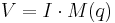
A memristor /ˈmɛmrɨstər/ (a portmanteau of "memory resistor") is a passive two-terminal circuit element in which the resistance is a function of the time history of the current and voltage through the device. Memristor theory was formulated and named by Leon Chua in a 1971 paper.[3]
On April 30, 2008 a team at HP Labs announced the development of a switching memristor. Based on a thin film of titanium dioxide, it has a regime of operation with an approximately linear charge-resistance relationship.[4][5][6] These devices are being developed for application in nanoelectronic memories, computer logic, and neuromorphic computer architectures.[7]
Contents |
Background

A memristor is a passive two-terminal electronic component for which the resistance (dV/dI) is proportional to the amount of charge that has flowed through the circuit. When current flows in one direction through the device, the resistance increases; and when current flows in the opposite direction, the resistance decreases. When the current is stopped, the component retains the last resistance that it had, and when the flow of charge starts again, the resistance of the circuit will be what it was when it was last active.[8].
More generally, a memristor is a two-terminal component in which the resistance depends on the integral of the input applied to the terminals, rather than on instantaneous value of the input at the terminals. Since the element "remembers" the amount of current that has passed through it in the past, it was tagged by Chua with the name "memristor." A general memristor is any of various kinds of passive two-terminal circuit elements that maintain a functional relationship between the time integrals of current and voltage. This function, called memristance, is similar to variable resistance. Specifically engineered memristors provide controllable resistance, but such devices are not commercially available. Other devices such as batteries and varistors have memristance, but it does not normally dominate their behavior. The definition of the memristor is based solely on fundamental circuit variables, similarly to the resistor, capacitor, and inductor. Unlike those three elements, which are allowed in linear time-invariant or LTI system theory, memristors are nonlinear and may be described by any of a variety of time-varying functions of net charge. There is no such thing as a generic memristor. Instead, each device implements a particular function, wherein either the integral of voltage determines the integral of current, or vice versa. A linear time-invariant memristor is simply a conventional resistor.[9]
In his 1971 paper, memristor theory was formulated and named by Leon Chua,[3] extrapolating the conceptual symmetry between the resistor, inductor, and capacitor, and inferring that the memristor is a similarly fundamental device. Other scientists had already proposed fixed nonlinear flux-charge relationships, but Chua's theory introduced generality.
Like other two-terminal components (e.g., resistor, capacitor, inductor), real-world devices are never purely memristors ("ideal memristor"), but will also exhibit some amount of capacitance, resistance, and inductance.
Theory
The memristor is essentially a two-terminal variable resistor, with resistance dependent upon the amount of charge q that has passed between the terminals.
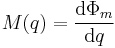
To relate the memristor to the resistor, capacitor, and inductor, it is helpful to isolate the term M(q), which characterizes the device, and write it as a differential equation.
| Device | Characteristic property (units) | Differential equation |
|---|---|---|
| Resistor | Resistance (A / V = Ω) | R = dI / dV |
| Capacitor | Capacitor (C / V = F) | C = dQ / dV |
| Inductor | Inductance (Wb / A = H) | L = dΦm / dI |
| Memristor | Memristance (Wb / C = Ω) | M = dΦm / dQ |
where Q is defined by Q = dI/dt, and Φm is defined by V = dΦm/dt. Note that the above table covers all meaningful ratios of I, Q, Φm, and V. No device can relate I to Q, or Φm to V, because I is the integral of Q and Φm is the integral of V.
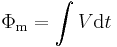
The variable Φm ("magnetic flux linkage") is a generalized from the circuit characteristic of an inductor. It does not represent a magnetic field here, and its physical meaning is discussed below. The symbol Φm may simply be regarded as the integral of voltage over time.[10]
Thus, the memristor is formally defined[3] as a two-terminal element in which the flux linkage (or integral of voltage) Φm between the terminals is a function of the amount of electric charge Q that has passed through the device. Each memristor is characterized by its memristance function describing the charge-dependent rate of change of flux with charge.
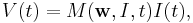
Substituting that magnetic flux is simply the time integral of voltage, and charge is the time integral of current, we may write the more convenient form
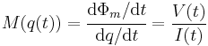
It can be inferred from this that memristance is simply charge-dependent resistance. If M(q(t)) is a constant, then we obtain Ohm's Law R(t) = V(t)/ I(t). If M(q(t)) is nontrivial, however, the equation is not equivalent because q(t) and M(q(t)) will vary with time. Solving for voltage as a function of time we obtain

This equation reveals that memristance defines a linear relationship between current and voltage, as long as M does not vary with charge. Of course, nonzero current implies time varying charge. Alternating current, however, may reveal the linear dependence in circuit operation by inducing a measurable voltage without net charge movement—as long as the maximum change in q does not cause much change in M.
Furthermore, the memristor is static if no current is applied. If I(t) = 0, we find V(t) = 0 and M(t) is constant. This is the essence of the memory effect.
The power consumption characteristic recalls that of a resistor, I2R.

As long as M(q(t)) varies little, such as under alternating current, the memristor will appear as a resistor. If M(q(t)) increases rapidly, however, current and power consumption will quickly stop.
Flux linkage in a passive device
In an inductor, magnetic flux Φm typically relates to Faraday's law of induction, which states that the energy to push charges around a loop (electromotive force, in units of volts) equals the negative derivative of the flux through the loop:

This notion may be extended by analogy to a single device. Working against an accelerating force (which may be EMF, or any applied voltage), a resistor produces a decelerating force, and an associated "flux linkage" varying with opposite sign. For example, a high-valued resistor will quickly produce flux linkage. The term "flux linkage" is more commonly used with inductors, where it makes more sense: If an average of 1 volt is applied across an inductor over 1 second, then there is 1 V·s of flux linkage in the inductor, which represents energy that may later be obtained from it. The same bias over the same time across a resistor results in the same flux linkage, but the energy is dissipated — there is no physical magnetic field involved as a link to anything. Voltage for passive devices is evaluated in terms of energy lost by a unit of charge, so generalizing the above equation simply requires reversing the sense of EMF.

Observing that Φm is simply equal to the integral over time of the potential drop between two points, we find that it may readily be calculated, for example by an operational amplifier configured as an integrator.
Two unintuitive concepts are at play:
- Magnetic flux is defined here as generated by a resistance in opposition to an applied field or electromotive force. In the absence of resistance, flux due to constant EMF, and the magnetic field within the circuit, would increase indefinitely. The opposing flux induced in a resistor must also increase indefinitely so the sum with applied EMF remains finite.
- Any appropriate response to applied voltage may be called "magnetic flux," as the term is used here.
The upshot is that a passive element may relate some variable to flux without storing a magnetic field. Indeed, a memristor always appears instantaneously as a resistor. As shown above, assuming non-negative resistance, at any instant it is dissipating power from an applied EMF and thus has no outlet to dissipate a stored field into the circuit. This contrasts with an inductor, for which a magnetic field stores all energy originating in the potential across its terminals, later releasing it as an electromotive force within the circuit.
Physical restrictions on M(q)
An applied constant voltage potential results in uniformly increasing Φm. Numerically, infinite memory resources, or an infinitely strong field, would be required to store a number which grows arbitrarily large. Three alternatives avoid this physical impossibility:
- M(q) approaches zero, such that Φm = ∫M(q)dq = ∫M(q(t))I dt remains bounded but continues changing at an ever-decreasing rate. Eventually, this would encounter some kind of quantization and non-ideal behavior.
- M(q) is periodic, so that M(q) = M(q − Δq) for all q and some Δq, e.g. sin2(q/Q).
- The device enters hysteresis once a certain amount of charge has passed through, or otherwise ceases to act as a memristor.
Memristive systems
The memristor was generalized to memristive systems in a 1976 paper by Leon Chua.[11] Whereas a memristor has mathematically scalar state, a system has vector state. The number of state variables is independent of, and usually greater than, the number of terminals.
In this paper, Chua applied this model to empirically observed phenomena, including the Hodgkin-Huxley model of the axon and a thermistor at constant ambient temperature. He also described memristive systems in terms of energy storage and easily observed electrical characteristics. These characteristics match resistive random-access memory and phase-change memory, relating the theory to active areas of research.
In the more general concept of an n-th order memristive system the defining equations are

where the vector w represents a set of n state variables describing the device.[12] The pure memristor is a particular case of these equations, namely when M depends only on charge (w=q) and since the charge is related to the current via the time derivative dq/dt=I. For pure memristors f is not an explicit function of I.[12]
Operation as a switch
For some memristors, applied current or voltage will cause a great change in resistance. Such devices may be characterized as switches by investigating the time and energy that must be spent in order to achieve a desired change in resistance. Here we will assume that the applied voltage remains constant and solve for the energy dissipation during a single switching event. For a memristor to switch from Ron to Roff in time Ton to Toff, the charge must change by ΔQ = Qon−Qoff.

To arrive at the final expression, substitute V=I(q)M(q), and then ∫dq/V = ∆Q/V for constant V. This power characteristic differs fundamentally from that of a metal oxide semiconductor transistor, which is a capacitor-based device. Unlike the transistor, the final state of the memristor in terms of charge does not depend on bias voltage.
The type of memristor described by Williams ceases to be ideal after switching over its entire resistance range and enters hysteresis, also called the "hard-switching regime."[13] Another kind of switch would have a cyclic M(q) so that each off-on event would be followed by an on-off event under constant bias. Such a device would act as a memristor under all conditions, but would be less practical.
Implementations
Titanium dioxide memristor
Interest in the memristor revived in 2008 when an experimental solid state version was reported by R. Stanley Williams of Hewlett Packard.[14][15][16] The article was the first to demonstrate that a solid-state device could have the characteristics of a memristor based on the behavior of nanoscale thin films. The device neither uses magnetic flux as the theoretical memristor suggested, nor stores charge as a capacitor does, but instead achieves a resistance dependent on the history of current.
Although not cited in HP's initial reports on their TiO2 memristor, the resistance switching characteristics of titanium dioxide was originally described in the 1960s.[17]
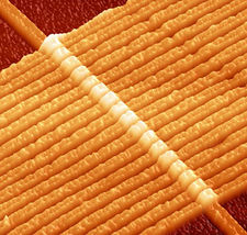
The HP device is composed of a thin (50 nm) titanium dioxide film between two 5 nm thick electrodes, one Ti, the other Pt. Initially, there are two layers to the titanium dioxide film, one of which has a slight depletion of oxygen atoms. The oxygen vacancies act as charge carriers, meaning that the depleted layer has a much lower resistance than the non-depleted layer. When an electric field is applied, the oxygen vacancies drift (see Fast ion conductor), changing the boundary between the high-resistance and low-resistance layers. Thus the resistance of the film as a whole is dependent on how much charge has been passed through it in a particular direction, which is reversible by changing the direction of current.[5] Since the HP device displays fast ion conduction at nanoscale, it is considered a nanoionic device.[18]
Memristance is displayed only when both the doped layer and depleted layer contribute to resistance. When enough charge has passed through the memristor that the ions can no longer move, the device enters hysteresis. It ceases to integrate q=∫Idt but rather keeps q at an upper bound and M fixed, thus acting as a resistor until current is reversed.
Memory applications of thin-film oxides had been an area of active investigation for some time. IBM published an article in 2000 regarding structures similar to that described by Williams.[19] Samsung has a U.S. patent for oxide-vacancy based switches similar to that described by Williams.[20] Williams also has a pending U.S. patent application related to the memristor construction.[21]
Although the HP memristor is a major discovery for electrical engineering theory, it has yet to be demonstrated in operation at practical speeds and densities. Graphs in Williams' original report show switching operation at only ~1 Hz. Although the small dimensions of the device seem to imply fast operation, the charge carriers move very slowly, with an ion mobility of 10−10 cm2/(V*s). In comparison, the highest known drift ionic mobilities occur in advanced superionic conductors, such as rubidium silver iodide with about 2×10⁻⁴ cm2/(V*s) conducting silver ions at room temperature. Electrons and holes in silicon have a mobility ~1000 cm2/(V*s), a figure which is essential to the performance of transistors. However, a relatively low bias of 1 volt was used, and the plots appear to be generated by a mathematical model rather than a laboratory experiment.[5]
In April 2010, HP labs announced that they had practical memristors working at 1ns switching times and 3 nm by 3 nm sizes, with electron/hole mobility of 1m/s[22] , which bodes well for the future of the technology.[23] At these densities it could easily rival the current sub-25 nm flash memory technology.
Polymeric memristor
In July 2008, Victor Erokhin and Marco P. Fontana, in Electrochemically controlled polymeric device: a memristor (and more) found two years ago,[24] claim to have developed a polymeric memristor before the titanium dioxide memristor more recently announced.
In 2004, Juri H. Krieger and Stuart M. Spitzer published a paper "Non-traditional, Non-volatile Memory Based on Switching and Retention Phenomena in Polymeric Thin Films"[25] at the IEEE Non-Volatile Memory Technology Symposium, describing the process of dynamic doping of polymer and inorganic dielectric-like materials in order to improve the switching characteristics and retention required to create functioning nonvolatile memory cells. Described is the use of a special passive layer between electrode and active thin films, which enhances the extraction of ions from the electrode. It is possible to use fast ion conductor as this passive layer, which allows to significantly decrease the ionic extraction field.
Spin memristive systems
Spintronic Memristor
Yiran Chen and Xiaobin Wang, researchers at disk-drive manufacturer Seagate Technology, in Bloomington, Minnesota, described three examples of possible magnetic memristors in March, 2009 in IEEE Electron Device Letters.[26] In one of the three, resistance is caused by the spin of electrons in one section of the device pointing in a different direction than those in another section, creating a "domain wall," a boundary between the two states. Electrons flowing into the device have a certain spin, which alters the magnetization state of the device. Changing the magnetization, in turn, moves the domain wall and changes the device's resistance.
This work attracted significant attention from the electronics press, including an interview by IEEE Spectrum.[27]
Spin Torque Transfer Magnetoresistance
Spin Torque Transfer MRAM is a well-known device that exhibits memristive behavior. The resistance is dependent on the relative spin orientation between two sides of a magnetic tunnel junction. This in turn can be controlled by the spin torque induced by the current flowing through the junction. However, the length of time the current flows through the junction determines the amount of current needed, i.e., the charge flowing through is the key variable.[28]
Additionally, as reported by Krzysteczko et al.,[29] MgO based magnetic tunnel junctions show memristive behavior based on the drift of oxygen vacancies within the insulating MgO layer (resistive switching). Therefore, the combination of spin transfer torque and resistive switching leads naturally to a second-order memristive system with w=(w1,w2) where w1 describes the magnetic state of the magnetic tunnel junction and w2 denotes the resistive state of the MgO barrier. Note that in this case the change of w1 is current-controlled (spin torque is due to a high current density) whereas the change of w2 is voltage-controlled (the drift of oxygen vacancies is due to high electric fields).
Spin Memrisitive System
A fundamentally different mechanism for memristive behavior has been proposed by Yuriy V. Pershin and Massimiliano Di Ventra in their paper "Spin memristive systems".[30] The authors show that certain types of semiconductor spintronic structures belong to a broad class of memristive systems as defined by Chua and Kang.[11] The mechanism of memristive behavior in such structures is based entirely on the electron spin degree of freedom which allows for a more convenient control than the ionic transport in nanostructures. When an external control parameter (such as voltage) is changed, the adjustment of electron spin polarization is delayed because of the diffusion and relaxation processes causing a hysteresis-type behavior. This result was anticipated in the study of spin extraction at semiconductor/ferromagnet interfaces,[31] but was not described in terms of memristive behavior. On a short time scale, these structures behave almost as an ideal memristor.[3] This result broadens the possible range of applications of semiconductor spintronics and makes a step forward in future practical applications of the concept of memristive systems.
Manganite memristive systems
Although not described using the word "memristor", a study was done of bilayer oxide films based on manganite for non-volatile memory by researchers at the University of Houston in 2001.[32] Some of the graphs indicate a tunable resistance based on the number of applied voltage pulses similar to the effects found in the titanium dioxide memristor materials described in the Nature paper "The missing memristor found".
Resonant tunneling diode memristor
In 1994, F. A. Buot and A. K. Rajagopal of the U.S. Naval Research Laboratory demonstrated[33] that a 'bow-tie' current-voltage (I-V) characteristics occurs in AlAs/GaAs/AlAs quantum-well diodes containing special doping design of the spacer layers in the source and drain regions, in agreement with the published experimental results.[34] This 'bow-tie' current-voltage (I-V) characteristic is characteristic of a memristor although the term memristor was not explicitly used in their papers. No magnetic interaction is involved in the analysis of the 'bow-tie' I-V characteristics.
3-terminal Memristor (Memistor)
Although the memristor is defined in terms of a 2-terminal circuit element, there was an implementation of a 3-terminal device called a memistor developed by Bernard Widrow in 1960. Memistors formed basic components of a neural network architecture called ADALINE developed by Widrow and Ted Hoff (who later invented the microprocessor at Intel). In one of the technical reports[35] the memistor was described as follows:
Like the transistor, the memistor is a 3-terminal element. The conductance between two of the terminals is controlled by the time integral of the current in the third, rather than its instantaneous value as in the transistor. Reproducible elements have been made which are continuously variable (thousands of possible analog storage levels), and which typically vary in resistance from 100 ohms to 1 ohm, and cover this range in about 10 seconds with several milliamperes of plating current. Adaptation is accomplished by direct current while sensing the neuron logical structure is accomplished nondestructively by passing alternating currents through the arrays of memistor cells.
Since the conductance was described as being controlled by the time integral of current as in Chua's theory of the memristor, the memistor of Widrow may be considered as a form of memristor having three instead of two terminals. However, one of the main limitations of Widrow's memistors was that they were made from an electroplating cell rather than as a solid-state circuit element. Solid-state circuit elements were required to achieve the scalability of the integrated circuit which was gaining popularity around the same time as the invention of Widrow's memistor.
A Google Knol article suggests that the Floating Gate MOSFET as well as other 3-terminal "memory transistors" may be modeled using memristive systems equations.[36]
Potential applications
Williams' solid-state memristors can be combined into devices called crossbar latches, which could replace transistors in future computers, taking up a much smaller area.
They can also be fashioned into non-volatile solid-state memory, which would allow greater data density than hard drives with access times potentially similar to DRAM, replacing both components.[37] HP prototyped a crossbar latch memory using the devices that can fit 100 gigabits in a square centimeter, and has designed a highly scalable 3D design (consisting of up to 1000 layers or 1 petabit per cm3).[7] HP has reported that its version of the memristor is currently about one-tenth the speed of DRAM.[38] The devices' resistance would be read with alternating current so that the stored value would not be affected.[39]
Some patents related to memristors appear to include applications in programmable logic,[40] signal processing,[41] neural networks,[42] and control systems.[43]
Recently, a simple electronic circuit[44] consisting of an LC network and a memristor was used to model experiments on adaptive behavior of unicellular organisms.[45] It was shown that the electronic circuit subjected to a train of periodic pulses learns and anticipates the next pulse to come, similarly to the behavior of slime molds Physarum polycephalum subjected to periodic changes of environment.[45] Such a learning circuit may find applications, e.g., in pattern recognition.
Memcapacitors and Meminductors
In 2009, Massimiliano Di Ventra, Yuriy Pershin and Leon Chua co-wrote an article[46] extending the notion of memristive systems to capacitive and inductive elements in the form of memcapacitors and meminductors whose properties depend on the state and history of the system.
Timeline of memristor and memristive systems developments
- 1960
- Bernard Widrow develops a 3-terminal device called a "memistor" as a new fundamental circuit component forming the basis of a neural network circuit called ADALINE (ADAptive LInear NEuron).
- 1967
- J.G. Simmons and R.R. Verderber publish an article in the Proceeding of the Royal Society of London entitled "New conduction and reversible memory phenomena in thin insulating films." The article notes hysteretic resistance switching effects in thin film (20-300 nm) silicon oxide having injected gold ions. Electron trapping is suggested as the explanation for the phenomena.
- 1968
- F. Argall publishes an article in Solid-State Electronics, Vol. 11, pp. 535–541 entitled "Switching Phenomena in Titanium Oxide Thin Films." Although the article is not cited in HP's memristor papers the article describes substantially similar experimental data.
- 1969
- G. Dearnaley A. M. Stoneham and D.V. Morgan 1969 J. Non Cryst. Sol. 4, 593 612 suggest the filamentary model for switching. They showed there were no injected gold ions in the silicon oxide films. Their 1970 paper G. Dearnaley A. M. Stoneham and D.V. Morgan 1970 Rep. Prog. Phys. 33, 1129 1191 reviewed and compared the several mechanisms proposed. This paper was translated into Russian as Uspekhi Fizicheskikh Nauk 112 83 128 (1974)
- 1971
- Leon Chua, a professor at UC Berkeley, postulates a new two-terminal circuit element characterized by a relationship between charge and flux linkage as a fourth fundamental circuit element in the article "Memristor-the Missing Circuit Element" published in IEEE Transactions on Circuit Theory.
- 1976
- Leon Chua and his student Sung Mo Kang publish a paper entitled "Memristive Devices and Systems" in the Proceedings of the IEEE generalizing the theory of memristors and memristive systems including a property of zero crossing in the Lissajous curve characterizing current vs. voltage behavior.
- 1986
- Robert Johnson and Stanford Ovshinsky receive U.S. Patent 4,597,162 describing manufacturing of a 2-terminal reconfigurable resistance switching array based on phase changing materials. While distinct from memristor behavior, some of the basic elements later used by Stan Williams group such as the use of a crossbar architecture and the basic use of a 2-terminal resistance switch are found in this patent.
- 1990
- S.Thakoor, A. Moopenn, T. Daud, and A.P. Thakoor publish an article entitled "Solid-state thin-film memistor for electronic neural networks" in the Journal of Applied Physics. The article teaches a tungsten oxide electrically reprogrammable variable resistance device but it is unclear whether the "memistor" referred to in the title has any connection to the memristor of Chua. In addition, the cited references of this article do not include any of Chua's publications on the memristor so this appears to be a coincidence.
- 1992
- Juri H. Krieger and Nikolai F. Yudanov receive RU. Patent 2,071,126 in the first describing application of a super-ionic material with high ion mobility for creating a resistance switching memory cell (August 27)
- 1993
- Ju. H. Krieger, N.F. Yudanov, I.K. Igumenov and S.B. Vaschenko publish an article entitled "Study of Test Structures of a Molecular Memory Element"[47] The article describe manufacturing of a resistance switching memory cell based on a conjugated polymer. (November 3)
- Katsuhiro Nichogi, Akira Taomoto, Shiro Asakawa, Kunio Yoshida of the Matsushita Research Institute receive U.S. Patent 5,223,750 describing an artificial neural function circuit formed using two-terminal organic thin film resistance switches which appear to have some properties similar to the memristor. However, no specific mention of memristors is made.
- 1994
- F. A. Buot and A. K. Rajagopal publish in the Journal of Applied Physics an article entitled "Binary information storage at zero bias in quantum-well diodes". The article demonstrates the existence of a memristor-'bow-tie' current-voltage characteristics in AlAs/GaAs/AlAs quantum-well diodes with special spacer-layer doping design. The analysis does not involve magnetic interaction and the authors were not aware of Chua's publications on memristor. It appears that the analysis bears no direct connection to the memristor of Chua.
- 1998
- Michael Kozicki and William West receive U.S. Patent 5,761,115 (assigned to Axon Technologies Corp. and the Arizona Board of Regents) describing the Programmable metallization cell, a device which consists of an ion conductor between two or more electrodes and whose resistance or capacitance can be programmed via the growth and dissolution of a metal "dendrite". No connection to memristors is made but the functionality is similar. (June 2)
- Bhagwat Swaroop, William West, Gregory Martinez, Michael Kozicki, and Lex Akers publish a paper entitled "Programmable Current Mode Hebbian Learning Neural Network Using Programmable Metallization Cell" in the Proceedings of the IEEE International Symposium on Circuits and Systems, (vol. 3, pp 33–36, 1998), demonstrating that the complexity of an artificial synapse can be minimized by using an ionic programmable resistance device. (June 3)
- James Heath, Philip Kuekes, Gregory Snider, and Stan Williams, of HP Labs, publish a paper in Science entitled "A Defect-Tolerant Computer Architecture:Opportunities for Nanotechnology." The article discusses how the possibility of a chemically fabricated 2-terminal configurable bit element can be implemented in a crossbar configuration and provide for defect tolerant computing. No connection to memristors is yet identified. (June 12)
- Ju. H. Krieger, N.F. Yudanov, I.K. Igumenov and S.B. Vaschenko publish an article entitled "Molecular Analogue Memory Cell" in the Proceedings of the Sixth Foresight Conference on Molecular Nanotechnology, Santa Clara, California, Nov. 12-15, 1998. (November 12)
- 2000
- A. Beck, J. G. Bednorz, Ch. Gerber, C. Rossel, and D. Widmer of IBM's Zurich Research Laboratory describe reproducible resistance switching effects in thin oxide films in the article "Reproducible switching effect in thin oxide films for memory applications" published in Applied Physics Letters. The switches are noted as having hysteretic features similar to memristors but no connection to memristors is yet noted. (July 3)
- Philip Kuekes, Stanley Williams, and James Heath, of HP Labs, receive U.S. Patent 6,128,214 (assigned to Hewlett-Packard) describing a nanoscale crossbar using a rotaxane molecular structure as a 2-terminal non-linear resistance switch. The connection to the memristor theory is not yet recognized. (October 3)
- 2001
- Shangqing Liu, NaiJuan Wu, Xin Chen, and Alex Ignatiev, researchers in the Space Vacuum Epitaxy Center of the University of Houston, present results during a non-volatile memory conference held in San Diego, California on Nov. 6-7 in the article "A New Concept for Non-Volatile Memory: The Electric Pulse Induced Resistive Change Effect in Colossal Magnetoresistive Thin Films." This appears to be the first identification of the importance of oxide bilayers to achieve a high to low resistance ratio. Data is provided indicative of the zero-crossing Lissajous curves discussed by Chua and Kang but no connection to memristors is yet noted and no explanation for the underlying mechanism is provided.
- Ju. H. Krieger, S.V. Trubin S.B., Vaschenko and N.F. Yudanov publish an article entitled "Molecular analogue memory cell based on electrical switching and memory in molecular thin films"[48] The article describe manufacturing of a two-terminal resistance switching array (8x8) based on a soluble oligomers of a conjugated polymer and an ionic complex (sodium salt). This principle allows creating memory cells with several bits per one cell and will allow working out the artificial neuron for neural networks and neural computers. (May 1)
- Ju. H. Krieger and N.F. Yudanov have a pending PCT International Application PCT/RU01/00334 describing memory cells having active and passive layers may store multiple information bits. The active layer may include conjugated polymers, an inclusion compounds or different type of oxide that have a variable resistance based on the movement of ions and electrons between the passive layer and the active layer. The passive layer may be a super-ionic material that has high ion and electron mobility. (August 13)
- 2004
- Ju. H. Krieger and N.F. Yudanov receive U.S. Patent 6,768,157 (July 27), 6,806,526 (October 19) 6,815,286 (November 9) (assigned to Advanced Micro Devices) describing memory cells having active and passive layers may store multiple information bits. The active layer may include conjugated polymers, an inclusion compounds or different type of oxide that have a variable resistance based on the movement of ions and electrons between the passive layer and the active layer. The passive layer may be a super-ionic material that has high ion and electron mobility.
- Ju. H. Krieger and Stuart M. Spitzer publish a paper in the IEEE Proceeding 2004 Non-Volatile Memory Technology Symposium entitled "Non-traditional, Non-volatile Memory Based on Switching and Retention Phenomena in Polymeric Thin Films". This work describes the process of dynamic doping of polymer and inorganic dielectric-like materials in order to improve the switching characteristics and retention required to create functioning nonvolatile memory cells. (15–17 November)
- 2005
- Darrell Rinerson, Christophe Chevallier, Steven Longcor, Wayne Kinney, Edmond Ward, and Steve Kuo-Ren Hsia receive U.S. Patent 6,870,755 (assigned to Unity Semiconductor) including basic patent claims to reversible 2-terminal resistance switching materials based on metal oxides. (March 22)
- Ju. H. Krieger and N.F. Yudanov receive U.S. Patent 6,838,720 (January 4) 6,855,977 (February 15), 6,858,481 (February 22), 6,864,522 (March 8), 6,873,540 (March 29) (assigned to Advanced Micro Devices) describing manufacturing of a two-terminal resistance switching memory cells having active and passive layers. Employing self-assembly produces polymer memory cells at the precise locations of the contacts of the transistor array. The mechanism of inducing the conductivity change of the polymer by changing its doping concentration provides a promising approach to make various memory devices.
- Zhida Lan, Colin Bill, and Michael A. VanBuskirk receive U.S. Patent 6,960,783 (assigned to Advanced Micro Devices) teaching a resistance switching memory cell formed from a layer of organic material and a layer of metal oxides or sulfides. The I-V characteristic (Fig. 14) is similar to the memristor but no mention of the memristor is included in the description. (November 1)
- 2006
- Stanford Ovshinsky receives U.S. Patent 6,999,953 describing a neural synaptic system based on phase change material used as a 2-terminal resistance switch. Leon Chua's original memristor paper is cited by the U.S. Patent Office as a pertinent prior art reference but no specific reference of connection to the memristor theory is made. (February 14)
- Ju. H. Krieger and N.F. Yudanov receive U.S. Patents 6,992,323 (January 31), 7,026,702 (April 11), 7,113,420 (September 26) (assigned to Advanced Micro Devices) describing manufacturing of a two-terminal resistance switching memory cells.
- Shangquig Liu, Naijuan Wu, Alex Ignatiev, and Jianren Li publish an article entitled "Electric-pulse-induced capacitance change effect in perovskite oxide thin films" which appears to disclose effects similar to that of a memcapacitor. (September 11)
- 2007
- Juri H. Krieger and Stuart M. Spitzer receive U.S. Patent 7,157,732 (assigned to Spansion describing manufacturing of a switchable diode with memory having a passive and active layer with asymmetric semiconducting properties. The active layer may include conjugated polymers, an inclusion compounds or different type of oxide that have a variable resistance based on the movement of ions and electrons between the passive layer and the active layer. The passive layer may be a super-ionic material that has high ion and electron mobility. (January 2)
- Vladimir Bulovic, Aaron Mandell, and Andrew Perlman, receive U.S. Patent 7,183,141 (assigned to Spansion), including basic claims to methods of programming 2-terminal ionic complex resistance switches to act as a fuse or anti-fuse. (February 27)
- Gregory Snider of HP Labs receives U.S. Patent 7,203,789, assigned to Hewlett-Packard, describing implementations of 2-terminal resistance switches similar to memristors in reconfigurable computing architectures. (April 10)
- Gregory Snider of HP Labs publishes the article "Self-organized computation with unreliable, memristive nanodevices" in the journal Nanotechnology discussing memristive nanodevices useful to pattern recognition and reconfigurable circuit architectures. (August 10)
- Blaise Mouttet, a graduate student at George Mason University, receives U.S. Patent 7,302,513 describing uses for 2-terminal resistance switching materials in signal processing, control systems, communications, and pattern recognition. (November 27)
- 2008
- Greg Snider of HP Labs receives U.S. Patent 7,359,888 (assigned to Hewlett-Packard) including basic claims to a nanoscale 2-terminal resistance switch crossbar array formed as a neural network. (April 15)
- Dmitri Strukov, Gregory Snider, Duncan Stewart, and Stan Williams, of HP Labs, publish an article in Nature "The missing memristor found"[49] identifying a link between the 2-terminal resistance switching behavior found in nanoscale systems and Leon Chua's memristor. (May 1)
- Blaise Mouttet, a graduate student at George Mason University, presents a poster entitled "Logicless Computational Architectures with Nanoscale Crossbar Arrays" describing analog computational architectures using 2-terminal resistance switching materials similar to the memristor at the 2008 NSTI Nanotechnology Conference and Trade Show in Boston. (June 1–5)
- Victor Erokhin and M.P. Fontana claim to have developed a polymeric memristor before the titanium dioxide memristor of Stan Williams group in the article "Electrochemically controlled polymeric device: a memristor (and more) found two years ago." (July 7)
- J. Joshua Yang, Matthew D. Pickett, Xuema Li, Douglas A. A. Ohlberg, Duncan R. Stewart and R. Stanley Williams publish an article in Nature Nanotechnology "Memristive switching mechanism for metal/oxide/metal nano-devices" demonstrating the memristive switching behavior and mechanism in nanodevices. (July 15)
- Stefanovich Genrikh, Choong-rae Cho, In-kyeong Yoo, Eun-hong Lee, Sung-il Cho, and Chang-wook Moon, receive U.S. Patent 7,417,271 (assigned to Samsung) including basic patent claims to a bilayer oxide 2-terminal resistance switch having memristive properties. However, the connection to Leon Chua's theory is not recognized in the patent description. (August 26)
- Blaise Mouttet, a graduate student at George Mason University, presents a poster entitled "Proposal for Memristors in Signal Processing" at Nano-Net 2008, a nanotechnology conference in Boston. (September 14–16)
- Yu V. Pershin and M. Di Ventra of UC San Diego publish an article in Physical Review Letters entitled "Spin memristive systems: Spin memory effects in semiconductor spintronics" which notes memristive behavior in spintronics. (September 23)
- Yu V. Pershin, S. La Fontaine, M. Di Ventra publish an article entitled "Memristive model of amoeba's learning" identifying memristive behavior in amoeba's learning. (October 22)
- Duncan Stewart, Patricia Beck, and Doug Ohlberg, researchers at HP Labs, receive U.S. Patent 7,443,711 (assigned to Hewlett-Packard) including basic patent claims to a tunable nanoscale 2-terminal resistance switch. (October 28)
- Blaise Mouttet, a graduate student at George Mason University, receives U.S. Patent 7,447,828 including various patent claims to using 2-terminal resistance switching materials in adaptive signal processing. (November 4)
- Leon Chua, Stan Williams, Greg Snider, Rainer Waser, Wolfgang Porod, Massimiliano Di Ventra, and Blaise Mouttet speak at a Symposium on Memristors and Memristive Systems held at UC Berkeley. Discussion includes the theoretical foundations of memristors and memristive systems of Leon Chua and Sung Mo Kang and the prospects of memristors for RRAM and neuromorphic electronic architectures. (November 21)
- Blaise Mouttet receives U.S. Patent 7,459,933 including various patent claims to using 2-terminal hysteretic resistance materials for image processing and pattern recognition. (December 2)
- 2009
- Sung Hyun Jo, Kuk-Hwan Kim, and Wei Lu of the University of Michigan publish an article in NanoLetters entitled "High-Density Crossbar Arrays Based on a Si Memristive System," which details an amorphous silicon based memristive material capable of being integrated with CMOS devices. (January 21)
- Massimiliano Di Ventra, Yuriy V. Pershin, Leon O. Chua submit an article in arXiv.org entitled "Circuit elements with memory: memristors, memcapacitors and meminductors" which extends the notion of memristive systems to capacitive and inductive elements, namely capacitors and inductors whose properties depend on the state and history of the system. (January 23, 2009)
- Blaise Mouttet published a Google knol article entitled: "An Introduction to Memimpedance and Memadmittance Systems Analysis"[50] which is an explanation on "Circuit elements with memory: memristors, memcapacitors and meminductors" and Chua's memristor paper. (January 30, 2009)
- HP Labs group publish an article entitled "A hybrid nanomemristor/transistor logic circuit capable of self-programming" in the Proceedings of the National Academy of Sciences. (February 10, 2009)
- An article is published in NanoLetters entitled "Nanoparticle Assemblies as Memristors" describing a newly discovered memristor material based on magnetite nanoparticles and proposing an extended memristor model including both time-dependent resistance and time-dependent capacitance. (May 1, 2009)
- Yuriy Pershin and Massimiliano Di Ventra published a preliminary article in Nature Precedings entitled "Experimental demonstration of associative memory with memristive neural networks" in which a memristor emulator demonstrates properties of a neural synapse. (May 19, 2009)
- A. Delgado published a paper entitled "Input Output Linearization of Memristive Systems" in the proceedings of the IEEE Nanotechnology Materials and Devices Conference; this work demonstrates that feedback linearization can be applied to the memristor producing a linear device. (June 2, 2009)
- Scientists at NIST published an article in IEEE Electron Device Letters entitled "A Flexible Solution-Processed Memristor". NIST's memristor is based on TiO2 like HPLabs but is fabricated using a less expensive room temperature deposition process and deposits the memristive material on flexible polymer sheets with potential applications as components of biosensors or RFID. (June 3, 2009)
- At the 2nd International Multi-Conference on Engineering and Technological Innovation, Blaise Mouttet of George Mason University described a memristor-based pattern recognition circuit performing an analog variation of the exclusive nor function. The circuit architecture is proposed as a way to circumvent Von Neumann's bottleneck for processors used in robotic control systems.[51] (July 13, 2009)
- The physical realization of an electrically modifiable array of memristive neural synapses is achieved by researchers at the Gwangju Institute of Science and Technology as reported in the journal Nanotechnology.[52] (August 4, 2009)
- Memristive behavior of magnetic tunnel junctions is reported by researchers from the Bielefeld University, Germany.[29] A combination of resistive and magnetoresistive switching leads to a second order memristive device. The two state variables are the state of the insulating layer (oxygen vacancy positions) and the state of the magnetic electrodes (the relative orientation of the magnetization direction). (September 17, 2009)
- 2010
- A review on memristor and its modeling approaches is accepted to be published in the Proceedings of the Royal Society A, preprint available at[53] (February, 17)
- The 2nd Memristor and Memristive Systems Symposium was held on Tuesday, February 2, 2010 at Sutardja Dai Hall, UC Berkeley.
- An array of memristors is demonstrated to perform logical functions.[54] (April 8)
- Memristor-based Content Addressable Memory (MCAM) is introduced and accepted in IEEE Transactions on Very Large Scale Integration (VLSI) Systems, it's currently available at[55] (April, 20)
- At the 2010 International Symposium on Circuits and Systems there were two special sessions on memristor devices and fabrication. One of the presentations entitled "The mythology of the memristor" by Blaise Mouttet argued that the interpretation of the memristor as a fourth fundamental was incorrect and that the device discovered by HPLabs was not actually a memristor but part of a broader class of memristive systems.[56] (June 1)
- HP announced they teamed up with Hynix to produce a commercial product dubbed "ReRam" August 31[57]
- 2013
- The first products using memristor technology are expected to become available.[58]
See also
- Integrated circuit
- List of emerging technologies
- RRAM
- Physical neural network
References
- ↑ Bush S, "HP nano device implements memristor", Electronics Weekly 2008-05-02
- ↑ Michael Kanellos "HP makes memory from a once-theoretical circuit" 2008-04-30 (Blog entry-not a reliable source)
- ↑ 3.0 3.1 3.2 3.3 Chua, Leon O (September 1971), "Memristor—The Missing Circuit Element", IEEE Transactions on Circuit Theory CT-18 (5): 507–519, doi:10.1109/TCT.1971.1083337, http://ieeexplore.ieee.org/xpls/abs_all.jsp?arnumber=1083337
- ↑ Tour, James M; He, Tao (2008), "Electronics: The fourth element", Nature 453 (7191): 42–43, doi:10.1038/453042a, PMID 18451847, http://www.nature.com/nature/journal/v453/n7191/full/453042a.html
- ↑ 5.0 5.1 5.2 Strukov, Dmitri B; Snider, Gregory S; Stewart, Duncan R; Williams, Stanley R (2008), "The missing memristor found", Nature 453 (7191): 80–83, doi:10.1038/nature06932, PMID 18451858, http://www.nature.com/nature/journal/v453/n7191/full/nature06932.html
- ↑ Marks, Paul (2008-04-30), Engineers find 'missing link' of electronics, New Scientist, http://technology.newscientist.com/article/dn13812-engineers-find-missing-link-of-electronics.html, retrieved 2008-04-30 See also: Researchers Prove Existence of New Basic Element for Electronic Circuits -- Memristor', Physorg.com, 2008-04-30, http://www.physorg.com/news128786808.html, retrieved 2008-04-30
- ↑ 7.0 7.1 'Missing link' memristor created, EETimes, 2008-04-30, http://www.eetimes.com/news/latest/showArticle.jhtml?articleID=207403521, retrieved 2008-04-30
- ↑ HP, Memristor FAQ (accessed Sept 3, 2010)
- ↑ Chua 1971, p. 511: ... In the very special case where the memristor Φ-q curve is a straight line, ... the memristor reduces to a linear time-invariant resistor.
- ↑ Knoepfel, Heinz (1970), Pulsed high magnetic fields, New York: North-Holland, pp. 37, Eq. (2.80).
- ↑ 11.0 11.1 Chua, L.O., and Kang, S.M., Memristive Devices and Systems, Proceedings of the IEEE 64, 209, 1976
- ↑ 12.0 12.1 Strukov, Dimitri B; Borghetti, Julien L.; Williams, R. Stanley (2009), "Coupled ionic and electronic transport model of thin-film semiconductor memristive behavior.", Small 5 (9): 1058–1063, doi:10.1002/smll.200801323, PMID 19226597
- ↑ Williams pp 81-82.
- ↑ Fildes, Jonathan (2007-11-13), Getting More from Moore's Law, BBC, http://news.bbc.co.uk/2/hi/technology/7080772.stm, retrieved 2008-04-30 See also: (PDF) Bulletin for Electrical and Electronic Engineers of Oregon, Institute of Electrical and Electronics Engineers, September 2007, http://www.ieee-or.org/beeep/2007/sep/beeep_sep07.pdf, retrieved 2008-04-30
- ↑ R. Stanley Williams (HP biography), http://www.hpl.hp.com/about/bios/stanwilliams.html
- ↑ Stan Williams, (HP biography), http://www.hpl.hp.com/research/qsr/people/Stan_Williams/
- ↑ Argall, F. (1968), "Switching Phenomena in Titanium Oxide Thin Films", Solid-State Electronics Vol. 11: 535–541, doi:10.1016/0038-1101(68)90092-0, http://pdf.com.ru/a/ky1300.pdf
- ↑ Terabe, Kazuya; Hasegawa, Tsuyoshi; Liang, Changhao; Aono, Masakazu (2007), "Control of local ion transport to create unique functional nanodevices based on ionic conductors", Science and Technology of Advanced Materials 8 (6): 536–542 (free download), doi:10.1016/j.stam.2007.08.002, http://linkinghub.elsevier.com/retrieve/pii/S146869960700126X
- ↑ Beck, A.; Bednorz, J.G.; Gerber, C.; Rossel, C.; Widmer, D. (2000), "Reproducible switching effect in thin oxide films for memory applications", Applied Physics Letters 77: 139, doi:10.1063/1.126902, http://link.aip.org/link/?APPLAB/77/139/1
- ↑ US Patent 7,417,271, http://patft.uspto.gov/netacgi/nph-Parser?Sect1=PTO1&Sect2=HITOFF&d=PALL&p=1&u=%2Fnetahtml%2FPTO%2Fsrchnum.htm&r=1&f=G&l=50&s1=7417271.PN.&OS=PN/7417271&RS=PN/7417271,
- ↑ US Patent Application 11/542,986, http://appft1.uspto.gov/netacgi/nph-Parser?Sect1=PTO2&Sect2=HITOFF&u=%2Fnetahtml%2FPTO%2Fsearch-adv.html&r=1&p=1&f=G&l=50&d=PG01&S1=20080090337.PGNR.&OS=dn/20080090337&RS=DN/20080090337,
- ↑ , http://www.youtube.com/watch?v=bKGhvKyjgLY
- ↑ , http://www.nytimes.com/2010/04/08/science/08chips.html?hpw
- ↑ Erokhin, V.; Fontana, M.P. (2008), "Electrochemically controlled polymeric device: a memristor (and more) found two years ago", Arxiv preprint, http://arxiv.org/pdf/0807.0333
- ↑ Juri H. Krieger and Stuart M. Spitzer, "Non-traditional, Non-volatile Memory Based on Switching and Retention Phenomena in Polymeric Thin Films", IEEE Proceeding 2004 Non-Volatile Memory Technology Symposium
- ↑ Wang, Xiaobin; Chen, Yiran; Xi, Haiwen; Dimitrov, Dimitor; Dimitrov, Dimitar (2009), "Spintronic Memristor through Spin Torque Induced Magnetization Motion", IEEE Electron Device Letters 30 (3): 294–297, doi:10.1109/LED.2008.2012270, http://ieeexplore.ieee.org/xpl/freeabs_all.jsp?isnumber=4787231&arnumber=4781542&count=31&index=28
- ↑ Savage, Neil (2009), "Spintronic Memristor through Spin Torque Induced Magnetization Motion", IEEE Spectrum (3), http://www.spectrum.ieee.org/semiconductors/devices/spintronic-memristors
- ↑ Y. Huai, AAPPS Bulletin, December 2008, vol. 18, No. 6, p. 33, "Spin-Transfer Torque MRAM (STT-MRAM): Challenges and Prospects."
- ↑ 29.0 29.1 Krzysteczko, Patryk; Günter, Reiss; Thomas, Andy (2009), "Memristive switching of MgO based magnetic tunnel junctions", Applied Physics Letters 95: 112508, doi:10.1063/1.3224193
- ↑ Pershin, Yuriy V; Di Ventra, Massimiliano (2008), "Spin memristive systems: Spin memory effects in semiconductor spintronics", Physical Review B 78: 113309, doi:10.1103/PhysRevB.78.113309, http://link.aps.org/abstract/PRB/v78/e113309
- ↑ Pershin, Yuriy V; Di Ventra, Massimiliano (2008), "Current-voltage characteristics of semiconductor/ferromagnet junctions in the spin-blockade regime", Physical Review B 77: 073301, doi:10.1103/PhysRevB.77.073301, http://link.aps.org/abstract/PRB/v77/e073301
- ↑ Liu, Shangqing; Wu, NaiJuan; Chen, Xin; Ignatiev, Alex (2001-11-06) (PDF), A New Concept for Non-Volatile Memory: The Electric Pulse Induced Resistive Change Effect in Colossal Magnetoresistive thin Films, http://klabs.org/richcontent/MemoryContent/nvmt_symp/nvmts_2001/papers_presentations/05_electric_pulse/05_Ignatiev-foils.pdf, retrieved 2008-10-05
- ↑ Buot, F. A.; Rajagopal, A. K. (1994), "Binary information storage at zero bias in quantum-well diodes", Journal of Applied Physics 76: 5552, doi:10.1063/1.357158
- ↑ Gullapalli,, K. K.; Tsao, D. P.; Neikirk,, D. P. (1993.), "Experimental observation of multiple current-voltage curves and zero-bias memory phenomena in quantum well diodes with n--n++- spacer layers", Applied Physics Letters 62: 2971, doi:10.1063/1.109160
- ↑ Widrow, B.; Pierce, W. H.; Angell, J.B. (1961), "Birth, Life, and Death in Microelectronic Systems", Technical Report No. 1552-2/1851-1, http://www-isl.stanford.edu/~widrow/papers/j1961birthlife.pdf
- ↑ Mouttet, Blaise. "An Extended Memristive System Model Applied to Floating Gate MOSFETs". http://knol.google.com/k/anonymous/an-extended-memristive-system-model/23zgknsxnlchu/8#. Retrieved 6 June 2010.
- ↑ Kanellos, Michael (2008-04-30), HP makes memory from a once theoretical circuit, CNET News.com, http://www.news.com/8301-10784_3-9932054-7.html, retrieved 2008-04-30
- ↑ Markoff, John (2008-05-01), H.P. Reports Big Advance in Memory Chip Design, NY Times, http://www.nytimes.com/2008/05/01/technology/01chip.html, retrieved 2008-05-01
- ↑ Gutmann, Ethan (2008-05-01), Maintaining Moore's law with new memristor circuits, Ars Technica, http://arstechnica.com/news.ars/post/20080501-maintaining-moores-law-with-new-memristor-circuits.html, retrieved 2008-05-01
- ↑ U.S. Patent 7,203,789
- ↑ U.S. Patent 7,302,513
- ↑ U.S. Patent 7,359,888
- ↑ US application 11/976,927
- ↑ Pershin, Yuriy V; La Fontaine, Steven; Di Ventra, Massimiliano (2009), "Memristive model of amoeba learning", Physical Review E 80: 021926, doi:10.1103/PhysRevE.80.021926, http://link.aps.org/doi/10.1103/PhysRevE.80.021926
- ↑ 45.0 45.1 Saigusa, Tetsu; Tero, Atsushi; Nakagaki, Toshiyuki; Kuramoto, Yoshiki (2008), "Amoebae Anticipate Periodic Events", Phys. Rev. Lett. 100 (1): 018101, doi:10.1103/PhysRevLett.100.018101, PMID 18232821, http://link.aps.org/abstract/PRL/v100/e018101
- ↑ Di Ventra, Massimiliano; Pershin, Yuriy V; Chua, Leon (2009), "Circuit elements with memory: memristors, memcapacitors and meminductors", Proceedings of the IEEE 97: 1717, doi:10.1109/JPROC.2009.2021077, http://ieeexplore.ieee.org/xpls/abs_all.jsp?isnumber=5247123&arnumber=5247127&count=13&index=7&tag=1
- ↑ Krieger, Ju. H.; Yudanov, N.F.; Igumenov, I.K.; Vaschenko, S.B. (1993), "Study of Test Structures of a Molecular Memory Element", Journal of Structural Chemistry 34 (6): 966–970, doi:10.1007/BF00752875
- ↑ Krieger, Ju. H.; Trubin, S.V.; Vaschenko, S.B.; Yudanov, N.F. (2001), "Molecular analogue memory cell based on electrical switching and memory in molecular thin films", Synthetic Metals 122: 199–202, doi:10.1016/S0379-6779(00)01354-0
- ↑ , http://www.nature.com/nature/journal/v453/n7191/full/nature06932.html
- ↑ http://knol.google.com/k/anonyme/an-introduction-to-memimpedance-and/23zgknsxnlchu/5
- ↑ Mouttet, Blaise L (2009), "Memristor Pattern Recognition Circuit Architecture for Robotics", Proceedings of the 2nd International Multi-Conference on Engineering and Technological Innovation II: 65–70, http://www.iiis2009.org/imeti/program/HTML/program-20.htm
- ↑ Choi, H; Jung, H; Lee, J; Yoon, J; Park, J; Seong, DJ; Lee, W; Hasan, M et al. (2009), "An electrically modifiable synapse array of resistive switching memory.", Nanotechnology 20 (34): 345201, doi:10.1088/0957-4484/20/34/345201, PMID 19652272, http://www.iop.org/EJ/abstract/0957-4484/20/34/345201
- ↑ . Kavehei, O.; Iqbal, A.; Kim, Y.S.; Eshraghian, K.; Al-Sarawi, S.F.; Derek, D. (2010), "The Fourth Element: Characteristics, Modelling, and Electromagnetic Theory of the Memristor", Proceedings of the Royal Society A: Mathematical, Physical and Engineering Sciences, http://arxiv.org/abs/1002.3210
- ↑ Borghetti, Julien (2010), "‘Memristive’ switches enable ‘stateful’ logic operations via material implication", Nature, http://www.nature.com/nature/journal/v464/n7290/full/nature08940.html
- ↑ . Eshraghian, K.; Cho, K.R.; Kavehei, O.; Kang, S.K.; Abbott, D.; Kang, S.M. (2010), "Memristor MOS Content Addressable Memory (MCAM): Hybrid Architecture for Future High Performance Search Engines", IEEE Transactions on Very Large Scale Integration (VLSI) Systems, http://arxiv.org/abs/1005.3687
- ↑ Mouttet, Blaise (2010), The mythology of the memristor, ISCAS, Paris, France, http://www.slideshare.net/blaisemouttet/mythical-memristor
- ↑ http://www.reuters.com/article/idUS254583059320100901
- ↑ http://www.technologyreview.com/computing/25018/?a=f
External links
- Hewlett Packard outlines computer memory of the future BBC News, Thursday, 8 April 2010
- Technical FAQ by Memristor lead scientist, Stan Williams of HP Labs May 20, 2008
- "Talk of the Nation" interview with co-discover Stan Williams of HP May 10, 2008
- HP Reveals Memristor, The Fourth Passive Circuit Element April 30, 2008
- BBC News - Electronics' 'missing link' found May 1, 2008
- Nature News - Found: the missing circuit element Apr 30, 2008
- Wired.com - Scientists Create First Memristor: Missing Fourth Electronic Circuit Element April 30, 2008
- EE Times - 'Missing link' memristor created: Rewrite the textbooks? April 30, 2008
- IEEE Spectrum - The Mysterious Memristor, by Sally Adee May 2008
- IEEE Spectrum - How We Found the Missing Memristor, by R. Stanley Williams Dec 2008
- Solid-state thin-film memristor for electronic neural networks - Journal of Applied Physics, vol. 67 March 1990
- A knol on memristors discussing applications in signal processing and filtering, artificial intelligence, computer/brain interfaces, etc.
- Memristive switching mechanism for metal/oxide/metal nanodevices July 15, 2008
- Java simulations of memristor circuits Dec 3, 2008
- Youtube video of 2008 Memristor and Memristive Systems Symposium at UC Berkeley
- Circuit elements with memory: memristors, memcapacitors and meminductors January 23, 2009
- An Introduction to Memimpedance and Memadmittance Systems Analysis
- A knol discussing companies involved in memristor electronics
- 6-minute memristor guide by R. Stanley Williams (Youtube) December 10, 2008 IEEE Spectrum online